

Oct. 26th
Low-Jitter RF-to-mm-Wave Frequency Generation
Abstract: Low-jitter local oscillator (LO) or clock signals from RF to mm-Wave frequencies are urgently demanded by high-speed communication and radar applications. In this talk, the performance limitation of the conventional charge-pump (CP) phase-locked loop (PLL) will be discussed first, illuminating the necessity of developing high-gain phase-detector (PD)-based PLL architectures. Then, the principle and performance metrics of analog PLLs based on the sampling and sub-sampling PDs and digital PLLs based on bang-bang PDs will be introduced. The state-of-the-art designs to achieve low jitter, low spur, and fast locking time will be shown afterward. The second part of this talk will focus on the mm-Wave frequency generation. The challenges and comparisons for various frequency plans will be presented first. Then, different solutions for synthesizing frequencies from 20GHz to 100GHz, including multi-stage PLL, frequency multiplication, and harmonic extraction, will be examined in detail, illustrating the most promising solution at each frequency band.
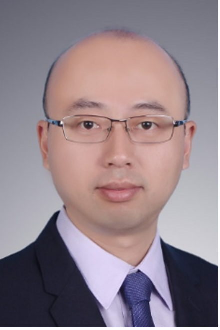
Speaker: Prof. Jun Yin, University of Macau
Jun Yin received the B.Sc. (2004) and the M.Sc. (2007) degrees in Microelectronics from Peking University, Beijing, China, and the Ph.D. (2013) degree in ECE from Hong Kong University of Science and Technology (HKUST), Hong Kong, China. He is currently an Associate Professor at the State Key Laboratory of Analog and Mixed-Signal VLSI, University of Macau, Macau, China. His research areas are circuits for high-speed communications and low-power IoTs. He authored or co-authored 1 book, 3 book chapters, and more than 90 peer-reviewed international conference and journal publications. He serves or has served on the TPCs for ISSCC, ESSERC, and A-SSCC. He was an Associate Editor of the TCAS-I.
Oct. 26th
Photonic-Electronic Convergence in Silicon-Based Optical Interconnect Chips
Abstract: The emerging AI computing asks for high bandwidth, high-density and low-power interconnects. The CMOS-compatible photonic-electronic converged Chiplet optical-I/O enables the large-scale multi-channel integration on chip. This talk focuses on the co-design techniques of silicon photonics and CMOS integrated electronics, exploring the promising techniques to achieve Tb/s per-chip bandwidth, pJ/bit power efficiency. The recent advances in this area will be reported, the technological trends will also be discussed.
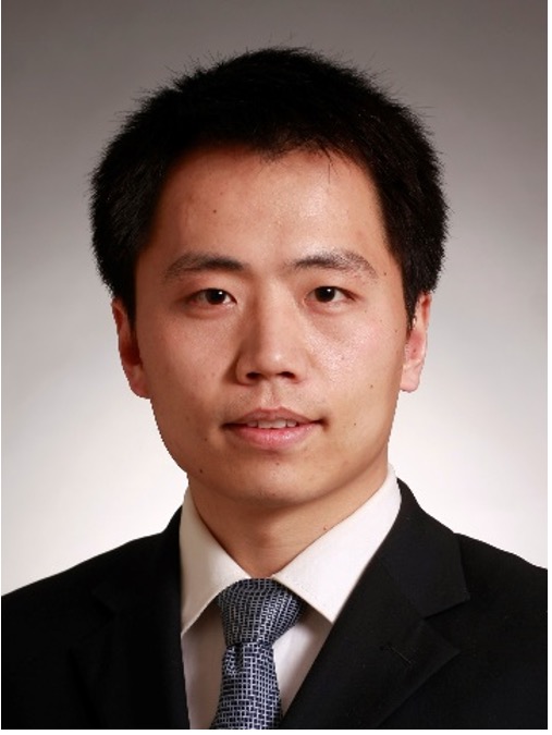
Speaker:Prof. Nan Qi, Institute of Semiconductors, Chinese Academy of Sciences
Nan Qi is a professor and PhD supervisor with the University of Chinese Academy of Sciences. He receives the PhD in Microelectronics from Tsinghua University in 2013. From 2013 to 2017, he was with Oregon State University, Corvallis, OR, and Hewlett-Packard Labs, Paloalto, CA, USA, respectively. Since 2017, he has been with the Institute of Semiconductors, Chinese Academy of Sciences, and the State Key Lab of Superlattices and Microstructures. His research focuses on the integrated circuits for optical communication, and photonic-electronic convergence communication chips. He has led more than 10 major projects including that granted by the NSFC and MOST. Dr Qi is a member of IEEE SSCS, CAS and Photonics, and has published more than 80 academic papers. He serves as a TPC member of IEEE ASSCC and ICTA.
Oct. 26th
Review and Outlook of Thermal Management in 3D Stacked IC Packaging
Abstract: It is well known that the carbon nanotubes (CNT) intrinsically have superior axial thermal conductivity. In the past, many research efforts attempted to apply CNT in electronic packaging to enhance the thermal performance of devices or modules. Nevertheless, even after 3 decades of presence of CNT, people still could not implement meaningful applications of CNT in the packaging of microelectronics. The present research intends to propose an innovative approach to make use of the superior axial thermal conductivity of CNT for heat conduction, in particular, for the thermal management application in 3D stacked IC packaging. We propose firstly to bond two substrates together with a fixed gap in between. This configuration will form two parallel surfaces. Subsequently two large areas of CNT will be grown simultaneously from the two parallel surfaces into each other. This face-to-face fabrication will bring CNT from the two sides to contact and eventually become interlaced. The interlaced CNT will provide better mechanical contacts and even allow some CNT from two sides to fuse together, becoming continuous CNT. These phenomena will certainly enhance the heat conduction between the two parallel surfaces. The configuration of parallel surfaces with a fixed gap happens to be the actual situation of 3D stacked chips. It is foreseeable that the outcome of the present research may lead to a revolution to the thermal management in 3D stacked IC packaging.
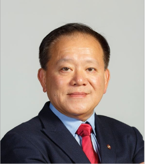
Speaker:Prof. Shi-Wei Ricky Lee, Hong Kong University of Science and Technology
Ricky Lee received his PhD degree in Aeronautical & Astronautical Engineering from Purdue University in 1992. Currently Dr Lee is Chair Professor in the Department of Mechanical and Aerospace Engineering at the Hong Kong University of Science and Technology (HKUST). He also has concurrent appointments as Dean of Systems Hub at the HKUST Guangzhou Campus and Director of Foshan Research Institute for Smart Manufacturing at HKUST. Dr Lee has been focusing his research on the technology development for electronics/optoelectronics packaging and additive manufacturing. The topics of his R&D interests include wafer level packaging and heterogeneous integration, 3D printing for microsystems packaging, LED packaging for solid-state lighting and applications beyond lighting, lead-free soldering and reliability analysis. In addition to being the recipient of 15 best/outstanding paper awards and 7 major professional society awards, Dr Lee is Fellow of IEEE, ASME, IMAPS, and Institute of Physics (UK). He also serves as the Editor-in-Chief of ASME Journal of Electronic Packaging.
Oct. 27th
Broadband mm-Wave Front-end for Radar and Wireless Communication
Abstract: At the mm-wave frequency, the broad bandwidth spectrum challenges the RF circuits on the specification of the bandwidth, gain, and efficiency. Those are design art and trade-offs for the RF-FE circuit, such as LNA, phase-shifter, and power amplifier. This talk will discuss a design methodology for broadband circuits, and a series of state-of-the-art circuits based on this design methodology will be presented.
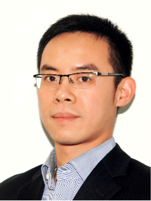
Speaker: Prof. Hao Gao, Southeast University / Eindhoven University of Technology
Dr. Gao graduated from TU Delft as an MSc, and TU Eindhoven with a Ph.D. degree in 2014. He was a Principal Scientist and Professor in the Silicon Austria Labs (SAL), a publicly funded national lab. He was with Philips Research Headquarters as a scientist, a European Marie Curie researcher in the NXP Stockholm, and a scientist/engineer/consultant at NXP semiconductor headquarters. Since 2014, Dr. Gao holds a professorship at the Eindhoven University of Technology, and now he is also a full professor in Southeast University with a National Chair. Dr. Gao served as a technical program committee member in the IEEE ISSCC, RFIC, ASSCC, ISSCC SRP, etc. He was a co-recipient of ISSCC 2015 Distinguished Technical Paper, San Francisco. He was also awarded the 2018 CATRENE Innovation Award, EU, with the EAST project.
Oct. 27th
Low Power Wireless Biopotential Sensor Design
Abstract: Biopotential signals acquisition plays a critical role in a human-computer interface system. Most of these biopotential signals distributed in the band of lower than kilo-hertz, or even lower than hundreds hertz. Precise acquisition of low amplitude signal at near DC frequency band is a challenge. In addition, the wearable/implantable scenario rises a high requirement in power efficiency, which causes a very limited power budget for the typically power hungry wireless data transmission. The existed commercial solutions, such as BLE and/or WiFi, are not suitable. This seminar first introduced the origins of various common vital signals, such as brain signals, heart signals, and etc. The key design concerns in the acquisition analog front end circuit and the wireless transmitter circuit are also introduced, with promising solutions. Demonstrations of frontier applications will also be shared by the end.
Speaker: Prof. Milin Zhang, Tsinghua University
Milin Zhang is an associate professor in the department of Electronic Engineering, Tsinghua University. She received the B.S. and M.S. degrees in electronic engineering from Tsinghua University, Beijing, China, in 2004 and 2006, respectively, and the Ph.D. degree in the Electronic and Computer Engineering Department, Hong Kong University of Science and Technology (HKUST), Hong Kong. After finishing her doctoral studies, she worked as a postdoctoral researcher at the University of Pennsylvania (UPenn). She joined Tsinghua University in 2016. Her research interests include sensor interface circuit and system design for biomedical applications and design of various non-traditional imaging sensors. She serves and has served as the Senior Associate Editor (SAE) of TCAS-II, Associate Editor (AE) of TBioCAS, the TPC member of ISSCC, CICC, A-SSCC and CASS. She is the Chapter chair of the SSCS Beijing chapter. She is the Distinguished Lecturer of CASS and IEEE WiE.
Oct. 27th
Emerging Electromagnetic Acoustic Sensing and Imaging beyond Radar and Ultrasound Systems
Abstract: Emerging Electromagnetic Acoustic technique is to combine the merits of traditional electromagnetic sensing technique (e.g. Radar and Lidar) with acoustic imaging (e.g. microphone and ultrasound), and go beyond. In this seminar, we would introduce three topics: (1) Low power phase arrayed Radar chip for SAR imaging, (2) Photoacoustics sensing and imaging system, (3) Thermoacoustics sensing system. On the phase array radar transceiver, the design challenge is to generate and transmit multiphased wideband chirp signal and to do stretch processing based high resolution beamforming. The detailed circuits and system to implement the radar sensor will be presented. Photoacoutics sensor transmit focused laser light deep penetrated to the tissue/blood vessel, inducing high frequency ultrasound signal, and then high resolution acoustic imaging can be formed. To miniaturize the whole sensor and achieve high sensitivity, the fibre coupled pulsed laser, beamforming ultrasound transducer, and low power low noise signal acquisition circuits are designed and implemented. Furthermore, there appears increasing interests to use microwave induced thermoacoustic and/or mageneto-acosutic signal for NDT applications. We will brief introduced some coil based EM transmitter for wireless power transfer, and EMAT based non-contact sensing.
Speaker: Prof. Zheng Yuanjin, Nanyang Technological University, Singapore
Dr. ZHENG Yuanjin received his B.Eng. from Xian Jiaotong University, P. R. China in 1993, M. Eng. from Xian Jiaotong University, P. R. China in 1996, and Ph.D. from Nanyang Technological University, Singapore in 2001. From July 1996 to April 1998, he worked at the national key lab of optical communication technology, university of electronic science and technology of China. He joined Institute of Microelectronics, A*STAR on 2001 and developed as a Group Technical Manager. Since then, he has leaded in developing various wireless systems and CMOS Integrated Circuits, such as Bluetooth, WLAN, WCDMA, UWB, RF SAW/MEMS Radar, wireless capsule imager etc. Since July 2009, he joined Nanyang Technological University, now a full professor, and as Director for Center of Integrated Circuits and Systems, and Director, Schaeffler-NTU Joint Lab working on various Sensor Systems. He has published over 500 papers, 5 book chapters and filed 30 patents, He has been granted total $45M to work on various R&D projects, including dozens of industrial projects. He serves as associate editor of IEEE transactions on Circuits and systems-I, IEEE Trans. on Biomedical Circuit and Systems, and IEEE Journal of Electromagnetics, RF and Microwave in Medicine and Biology. He is a senior member of IEEE, SPIE and OSA.


icta
All questions or inquiries for further information regarding ICTA should be directed to the Conference Secretariat at:
Tel: +86-10-66026729
+86-10-66024492
Email: contact@ieee-icta.net
© Copyright (2024) ICTA All rights reserved
China is rapidly emerging as a global hub for the semiconductor industry, encompassing academia, industry, and market growth. However, young Chinese researchers, especially students, often lack opportunities to participate in IEEE conferences. Meanwhile, international peers are eager to gain firsthand insights into China’s rapidly expanding semiconductor sector. In response to these needs, ICTA was established by a group of Chinese scholars and will be held annually in China. It aims to serve as a comprehensive and advanced forum for showcasing IC design, technologies, and applications on a global scale.
- Call For Paper
- Agenda
- Submission
- Registration
- Program
- Past Conference
- Committee
- Contacts